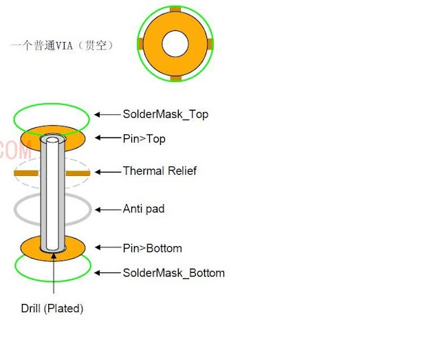
1. thermal relief:used instead of regular pads absorb heat conducted through connect lines, thermal relief can be : a. a negative pad on a positive copper area(shape).the thermal relief may be plotted as a regular pad flash(circle)with two line.b. a positive pad on an embedded metal layer that distributes a voltage, such as power or ground.
2. anti pad: negative pads, usually a circle , to prevent connection of a pin to an embedded metal layer.3. flash: user defined name of aperture for Gerber flashing of unique pad shape.
vic1689 發表在
痞客邦
留言(0)
人氣()
 Signal Layer and Positive Plane
Track to track :之間的最小要求間距Track to pad : 之間的最小要求間距Pad to pad : 之間的最小要求間距Pad to drill : 檢查pad是否在指定的數量的一定大小的drill有壞孔
vic1689 發表在
痞客邦
留言(0)
人氣()
vic1689 發表在
痞客邦
留言(0)
人氣()
vic1689 發表在
痞客邦
留言(0)
人氣()
vic1689 發表在
痞客邦
留言(0)
人氣()
vic1689 發表在
痞客邦
留言(0)
人氣()

下圖為軟硬結合版2層硬版+一條FPC.
vic1689 發表在
痞客邦
留言(0)
人氣()
●以10mil 單鍵變更來舉例:
在15.5 version 語法: funckey 1 options line_width 10
在16.3 version 語法: funckey 1 options acon_line_width 10
vic1689 發表在
痞客邦
留言(0)
人氣()

● IC's power and ground pin bypass CAP and fan-out 在類比與數位會有所不同,bypass cap主要的
功能,將high-frequency noise short to ground。
fan-out via 如下圖
1.bypass cap ground via距離PAD 越近越好。
vic1689 發表在
痞客邦
留言(0)
人氣()
 ●
●Placement 如何在工作環境上直接顯示component 高度,增加placement 效率.
1.Display / property
2.
3.
vic1689 發表在
痞客邦
留言(0)
人氣()

routing 的時候遇到內層PAD 需要NULL才能出線,NULL PAD 會有以下的工程問題需要注意。
vic1689 發表在
痞客邦
留言(0)
人氣()

allegro 16.3 如何自訂調色盤,如下圖
1.進入color 192 ,下方調色盤顏色也會套用到assign color,先找尋在pcbenv 底下有份檔案 color192.col若找不到可以在此畫面左上 file/save color palette..。
2. 進入customize 可調整自己需要的色調,將紅黃藍的參數記下。
3.開啟allegro192.col 即可修改裡面的顏色參數。
vic1689 發表在
痞客邦
留言(0)
人氣()


